2025-07-18
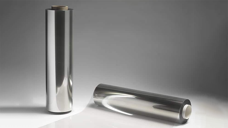
A Transparent Conductive Film (TCF) is a class of thin‐film materials that uniquely combine high electrical conductivity with optical transparency in the visible spectrum. As essential components in optoelectronic devices—such as touchscreens, displays, solar cells, smart windows, and flexible electronics—TCFs enable the flow of electric current while allowing light to pass through with minimal loss.
Composition & Properties
ITO is the most mature TCF technology, composed of ~90% indium oxide and 10% tin oxide. Its crystalline lattice features oxygen vacancies and Sn⁴⁺ dopants that furnish high carrier concentrations and sheet resistances typically from tens to hundreds of Ω/sq, with visible‐light transmittance around 80–90%. Post‐deposition annealing can further optimize both conductivity and transparency.
Limitations
ITO’s brittleness restricts its use in flexible or curved substrates, and increased film thickness (to lower sheet resistance) inevitably reduces transparency and risks film cracking under mechanical stress.
Structurea & Advantages
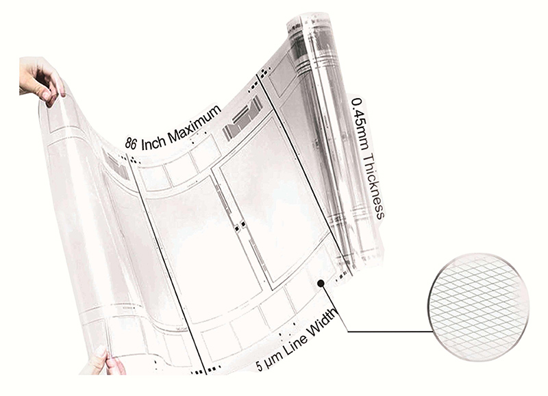
Metal‐mesh TCFs pattern ultrafine metal lines (e.g., Cu, Ag) into grid geometries on transparent substrates. This approach achieves very low sheet resistances (<10 Ω/sq), high transparency (>90%), and excellent mechanical robustness. Such films are ideal for applications requiring both large‐area coverage and flexibility—like transparent antennas, heated windows, and curved displays .
Challenges
Controlling line width below a few micrometers is critical to suppress Moiré patterns and maintain uniform optical performance, but this precision raises fabrication complexity and cost
Performance
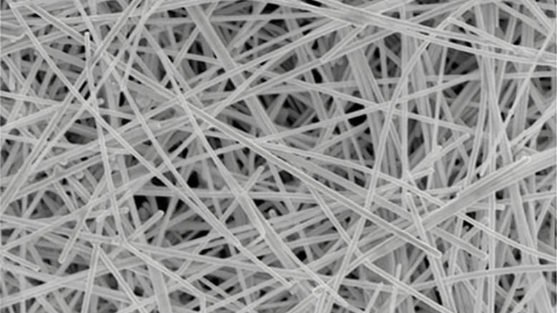
Networks of percolating silver nanowires deliver sheet resistances as low as 15 Ω/sq with transmittance above 90%. They exhibit superior flexibility compared to ITO and are produced via solution‐based processes, facilitating roll‐to‐roll printing for large‐scale manufacturing.
Stability Considerations
Silver is prone to oxidation and sulfuration; encapsulation layers or protective coatings are often required to ensure long‐term stability, at the expense of additional processing steps and costs.
Graphene’s atom‑thin structure confers exceptional electrical conductivity (~10⁴ S/cm) and optical transmittance (~97.7% per layer). Its mechanical strength and flexibility make it a promising ITO alternative for next‑generation flexible electronics.
Recent Advances
Composite TCFs: Hybrid films combining graphene with silver nanowires or conductive polymers (e.g., PEDOT:PSS) have achieved sheet resistances below 30 Ω/sq with >88% transmittance, alongside improved mechanical durability and moisture resistance
ACS Material.
Layer‑by‑Layer Assembly: Innovations in CVD growth and Langmuir–Blodgett techniques enable large‑area, few‑layer graphene films with uniform conductivity, suitable for photovoltaics and OLED electrodes
Nature.
PEDOT:PSS is a transparent, conductive polymer renowned for its ductility. When doped with high‑boiling‑point solvents (e.g., DMSO, sorbitol), its conductivity can rival that of metal oxides, while maintaining >85% transparency. It is widely used in antistatic coatings, OLEDs, and organic photovoltaics.
1. Magnetron Sputtering: Employs plasma to eject target atoms onto substrates under vacuum, widely used for ITO and metal films.
2. Chemical Vapor Deposition (CVD): Gaseous precursors react at elevated temperatures to deposit materials like graphene or metal oxides.
3. Evaporation: Thermal or e‐beam evaporation transfers source material to substrate in a vacuum chamber.
4. Solution Processing & Printing: Includes spin‐coating, spray‐coating, inkjet, and roll‐to‐roll printing—key to scalable production of AgNW and polymer‐based TCFs.
5. Etching & Patterning: Photolithography or laser ablation creates fine metal‐mesh geometries for advanced TCF designs.
Touchscreens & Displays
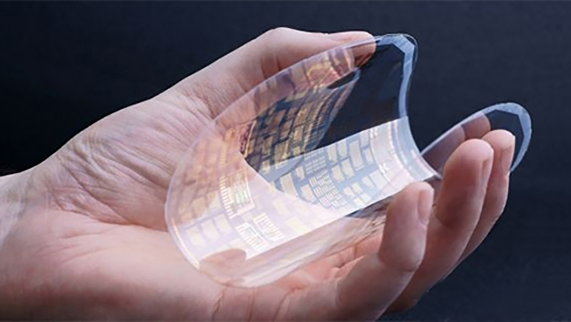
TCFs serve as transparent electrodes in smartphones, tablets, and large‐format touch panels. Graphene and AgNW films are gaining traction for foldable and rollable devices due to superior flexibility.
Photovoltaics & Solar Cells
Transparent electrodes collect and transport photovoltaic charges. Emerging graphene and metal mesh films aim to replace ITO in perovskite and organic solar cells, offering cost and flexibility advantages.
Smart Windows & Heating Elements
TCFs integrated into electrochromic and thermochromic windows enable dynamic control of light transmission. Metal‐mesh and AgNW films also power transparent heating panels to prevent condensation and ice formation on architectural glass and vehicle windshields.
Biomedical & Optical Instruments
In microscopy, biosensors, and lab‐on‐a‐chip systems, transparent electrodes permit simultaneous electrical stimulation and optical observation. PEDOT:PSS and graphene composites are prominent for their biocompatibility and flexibility.
MICRON delivers cutting-edge solutions based on copper metal mesh technology, including touch films, transparent antennas, transparent heating films, and EMI shielding films. Holding over 60% of global patents in metal mesh technology, we are committed to innovation, backed by a dedicated R&D team and stringent quality control to ensure product durability and reliability.
As a trusted supplier to leading global touch device manufacturers, MICRON has established subsidiaries in countries such as the United States and Japan to provide timely and efficient services worldwide, ensuring seamless support for our international clients.


