MiniLED, also known as sub-millimeter light-emitting diode, refers to an LED with a grain size of about 50-200 μm, whose grain size and dot pitch are between traditional small-pitch LED and MicroLED.
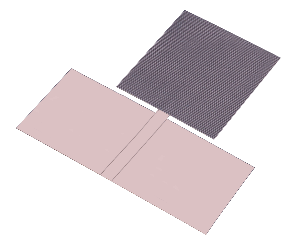
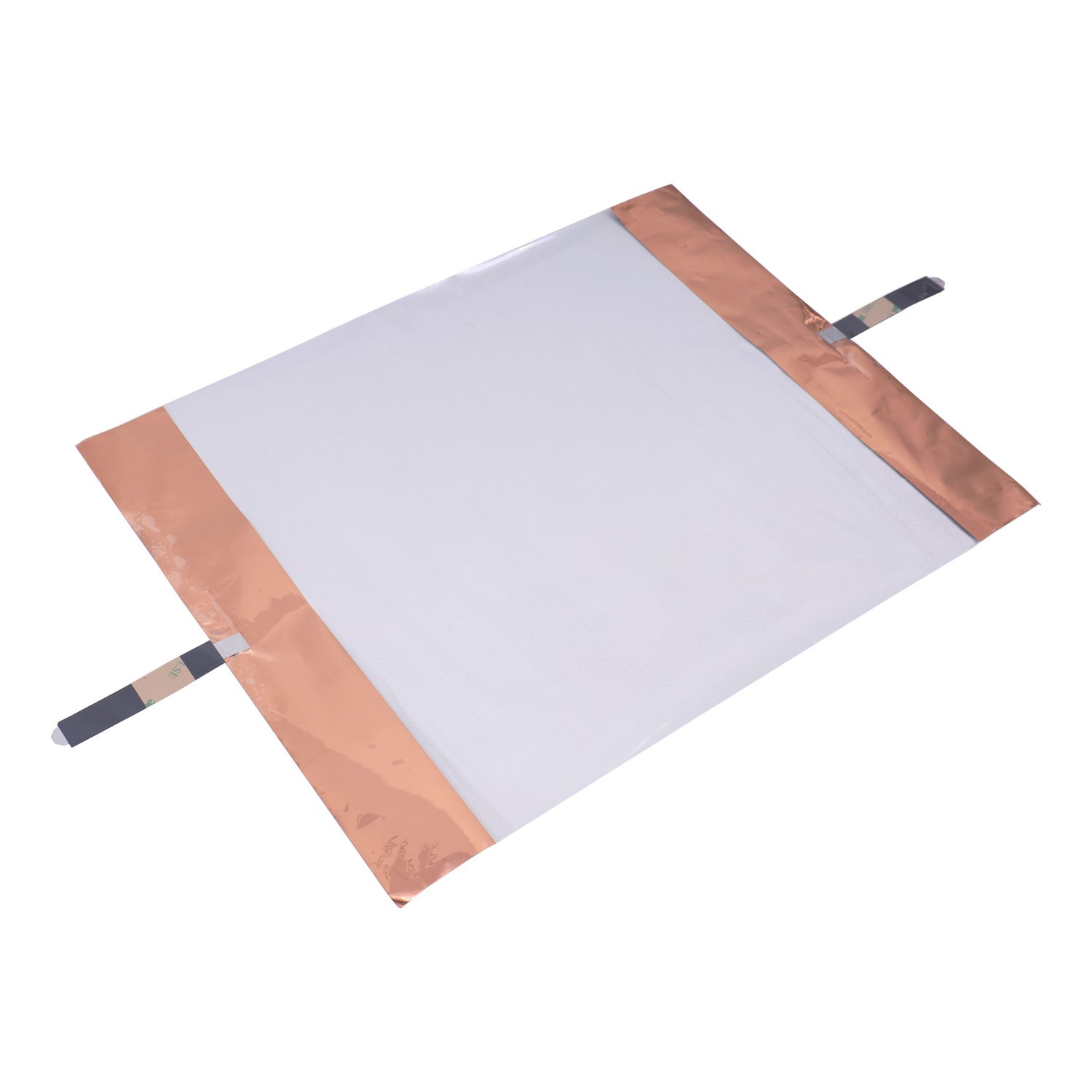
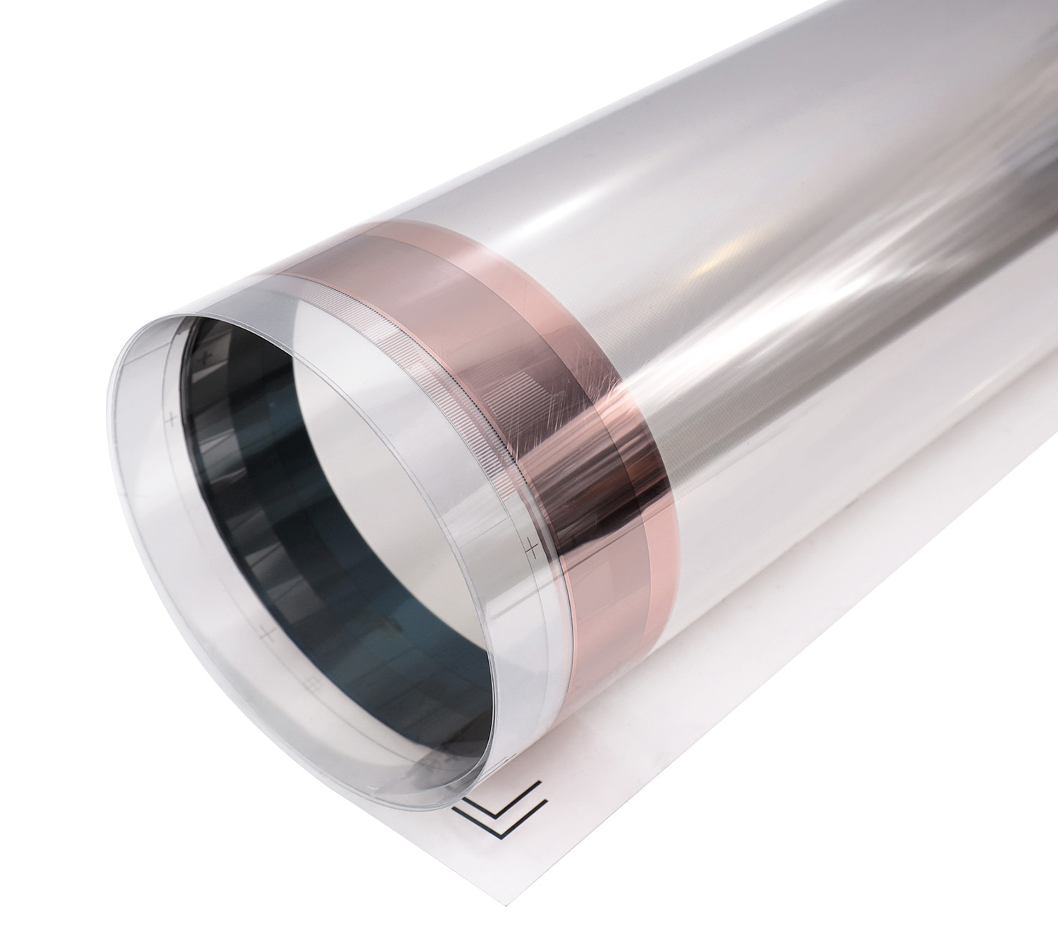
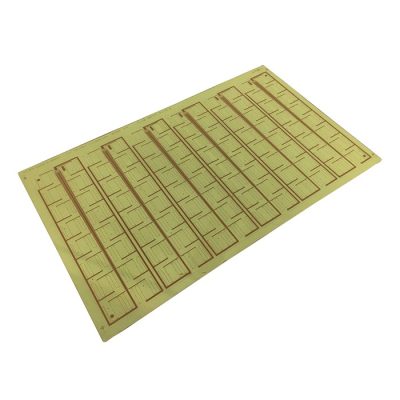
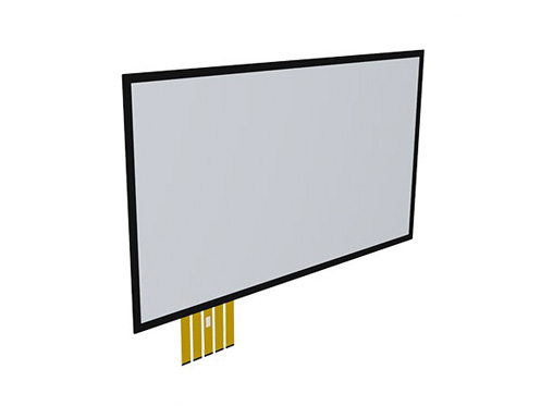
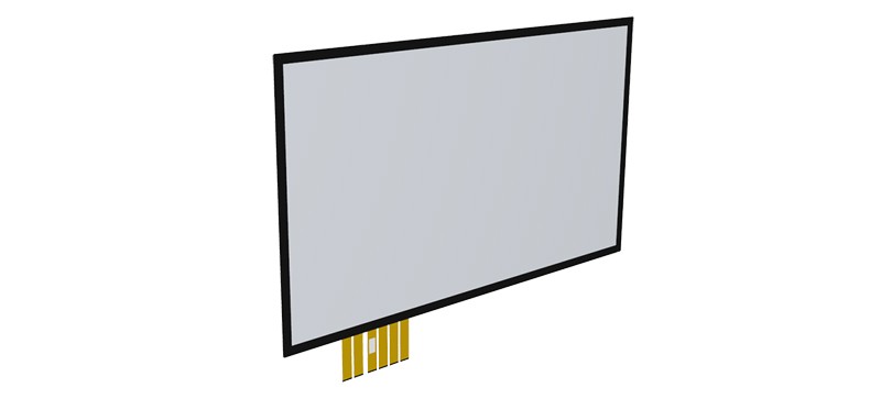
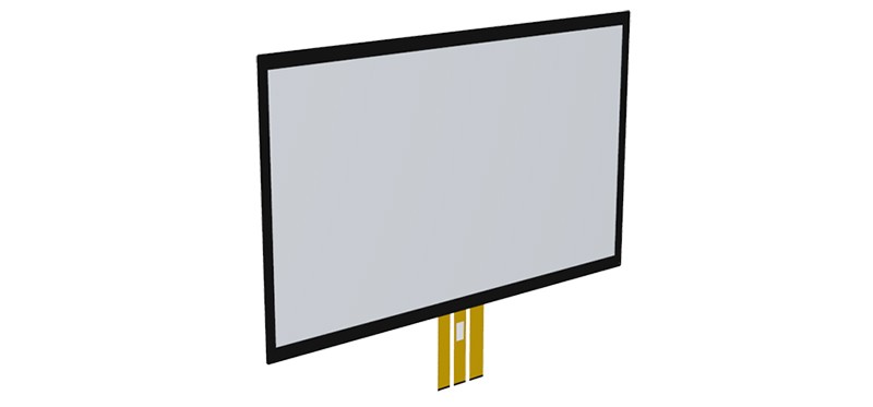
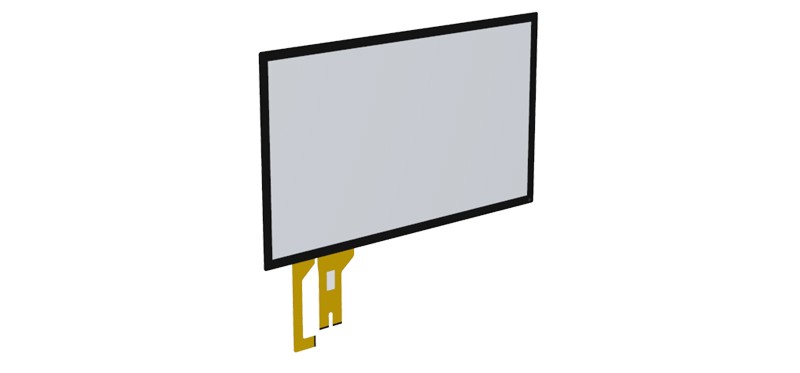
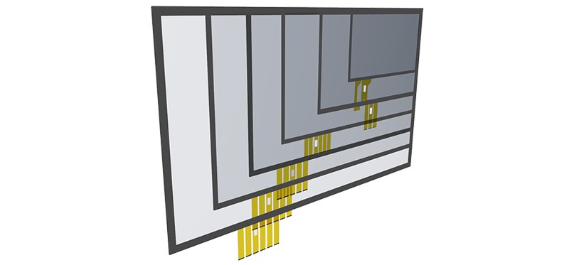
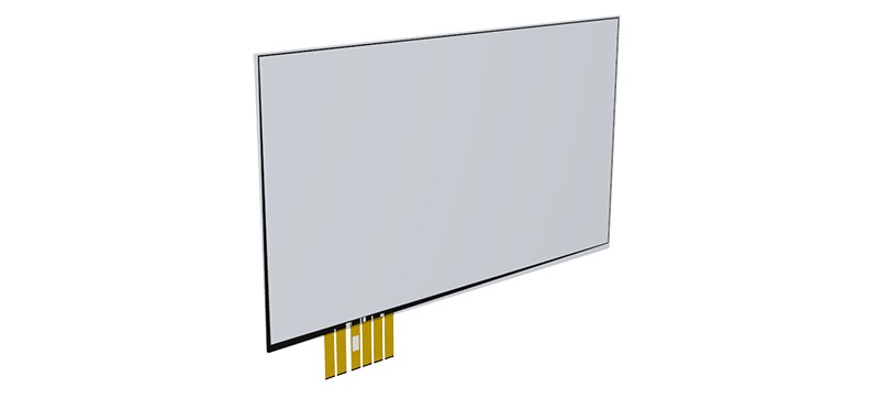
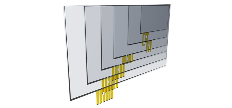
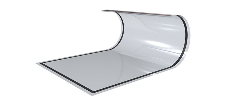
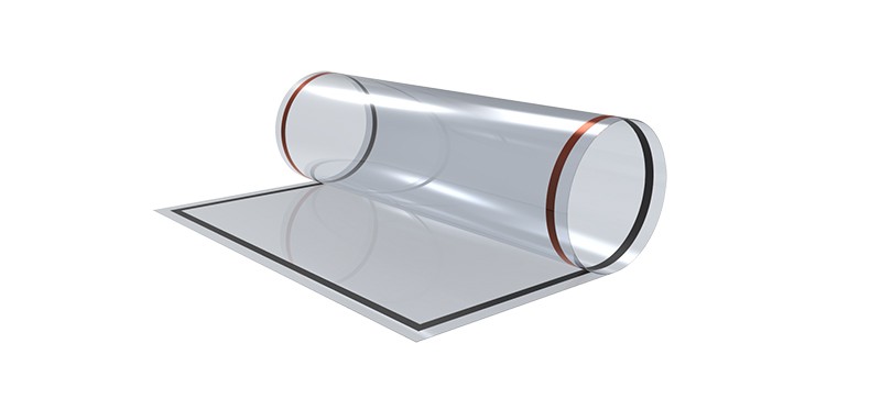
MiniLED is a composite design of embedded metal mesh touch elements, including MiniLED flexible substrate layer, MiniLED electrode layer, and chip layer, which are set on a heat shrinkable film substrate. The conductive materials include metal mesh, nano-silver, etc. The shrink film can be wrapped on the spherical support after heating, and finally matched with a flexible printed circuit board to achieve the function of multi-point spherical touch. Our products are mainly used for MiniLED drive circuits, which are etched on the substrate by yellow light method.
Customization.
(For example: high reflective material, any thickness copper films, PET/BT/Glass substrate, supports 50um-2mm thickness substrate, etc.).
Thin line width Process.
(L/S=40um/40um; copper thickness 12-15um).
The expansion and contraction of materials can be controlled within 6/10,000.
The size can support up to 2000*1250mm.
Flexible and foldable materials and IC solutions.
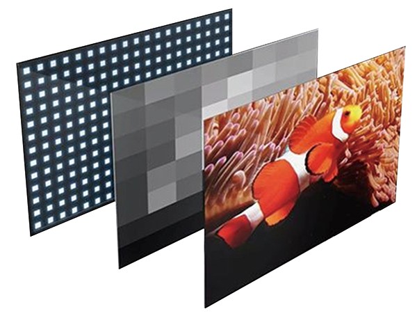
TV Backlight Applications
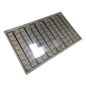
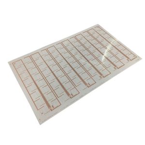
Mini LED Backlight Board Material – Glass Substrate and PCB Substrate.
Advantages
Limited by its own size and SMT mounting equipment, the size of the light board of the PCB substrate is small, Large-sized products require multiple light panels to be spliced and assembled, which affects the display quality. The glass substrate is a thin glass sheet with an extremely flat surface.
Glass substrate due to the high flatness of the board to support large size heat dissipation is better than PCB is the future development trend.
The core material of the glass substrate and the LED crystal are both inorganic semiconductor crystals, and the glass material is easier to achieve ultra-thin processing.
In the fields of high partition design such as VR wearable devices and mobile phone displays, the requirements for heat dissipation are higher, and the yield rate of small-sized glass-substrate production is acceptable.
Therefore, glass substrates have certain advantages. In addition, for high-density assembly, the flatness of the substrate is required, and the glass substrate is also a better choice.
The PCB substrate process technology is mature, and the high toughness of the copper material can effectively improve the straight yield.
The technical development of PCB substrates is more mature, and the supply chain is relatively complete. Its production yield is increasing year by year, and it is now well guaranteed.
However, glass-substrate products are fragile, and the maturity of the industry is relatively low. Therefore, the yield rate of glass-based MiniLED products at this stage is much lower than that of PCB-based MiniLED products.
Disadvantages
The larger size of the glass substrate, the more fragile it is, resulting in a lower production yield. Therefore, in the field of medium and large size, the glass substrate cannot compete with the PCB substrate. The material cost of the PCB substrate is several times that of the glass substrate. Due to the limitation of its own heat dissipation, the PCB substrate is easily warped and deformed in large-scale applications, which makes it more difficult to transfer MiniLED chips to the PCB substrate.
◆ VR, wearable devices and mobile phone display;
◆ Car monitors, pads, laptops, gaming monitors;
◆ TV, professional conference machine.
After years of precipitation and accumulation, our company has a complete R&D and production system to provide customers with overall solutions.
According to the design plan and requirements, we provide personalized customized services. We always adhere to the customer-oriented approach and tailor-made the best solution for customer needs.


-2.jpg)
-2.jpg)
-1.jpg)