2022-08-16
A circuit board explicitly made for compact electrical devices is known as a MiniLED substrate. It is one of the semiconductor industry’s leading providers of acceptable circuit processing solutions. The substrate is etched using an optimized etch chemistry which gives excellent results with low RIE bias and ultra-fast etches.
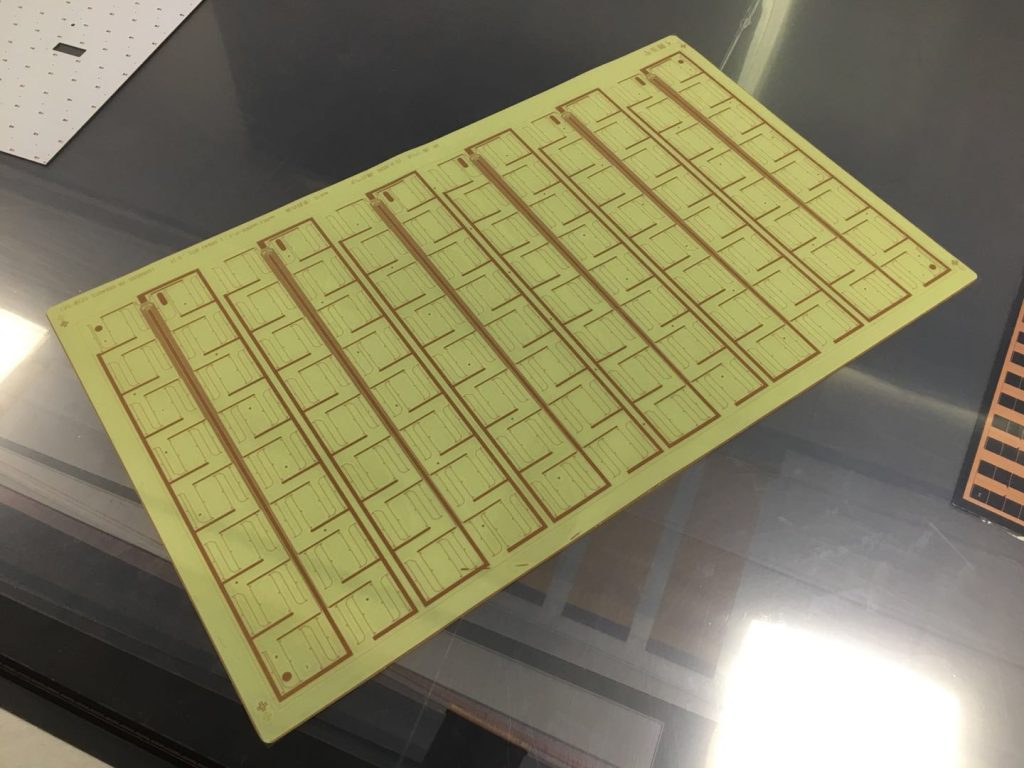
Fine circuit processing is a new method for manufacturing delicate circuits on flexible substrates. We have developed a novel process for fabricating high-quality and low-cost circuits using a combination of additive and subtractive processes. It is a next-generation substrate fine circuit processing technology that offers many benefits over traditional techniques. These materials have excellent thermal stability, mechanical strength, electrical insulation, and other characteristics. They also provide a wide choice of processing methods, such as etching, sputtering and electroplating. It allows you to print tiny circuits on plastic substrates.
What are the benefits of using MICRON MiniLED substrate Fine Circuit Processing?
Modern technology has several advantages over traditional substrates. The most notable benefits are the following:
A substrate plays a vital role in the fabrication process of electronic devices. It provides a stable base on which to build circuits or other components. A MiniLED substrate, also known as a sub-millimetre light-emitting diode, is an LED with grain size and dot pitch that falls between a typical small-pitch LED and a Micro LED. It is a composite design with integrated metal mesh touch components, mounted on a heat shrinkable film substrate, with a MiniLED flexible substrate layer, electrode layer, and chip layer.
The conductive materials include silver nanoparticles, metal mesh, etc. After heating, the shrink film may be wrapped around the spherical support and combined with a flexible printed circuit board to provide a multi-point spherical touch function. These items are etched onto the substrate using the yellow light technique. The substance utilized in these substrates has excellent mechanical qualities and high mechanical strength and is resistant to oil, fat, diluted alkali, diluted acid, and most solvents. It also has excellent transparency, UV blocking, and a nice gloss. These substrates are made from high-quality materials and are easy to process. Today, there has been a tremendous increase in demand for new types of substrates.
The characteristics of MiniLED Substrate Fine Circuit Processing
Cost-effective:
It is an innovative technology that enables the production of high-quality microelectronics components with minimal amounts of materials. It has a wide range of applications in the electronics industry. MiniLED Substrate Fine Circuit Processing can be used to produce high-quality microelectronics devices such as sensors, actuators, transistors, etc. The demand for miniaturized electronic products has overgrown in the electronics industry over the past few years. However, traditional methods have proven to be expensive and time-consuming. With the help of MiniLED Substrate Process Technology, we can manufacture high-quality microelectronic components more efficiently and cost-effectively. Our team of experts has developed it. When compared to other substrates, our substrates are cheaper and easier to handle. These Fine Substrate Circuits have been designed to provide ultra-thin substrates for next-generation electronics.
Increased production yields:
MiniLED Substrate Fine Circuit Processing is an innovative technology that allows the cost-effective processing of fine circuit boards. Our high-quality substrates will enable us to produce a wide range of fine circuit boards and electronic components. The main advantage of using MiniLED Substrate process technology is its ability to reduce material usage by up to 95%. MiniLED Substrates provide many benefits, including reduced footprint, improved yield, increased throughput and lower costs. We offer you a large variety of substrates, which enables us to provide you with customized solutions for your needs. They have been used in many industries such as aerospace, automotive, medical, etc.
High partition design:
The future development tendency is toward PET substrate since it supports considerable size heat dissipation better than PCB due to the board’s high flatness. Both the glass substrate and the LED crystal’s core components are inorganic semiconductor crystals, although glass is more accessible to produce an ultra-thin layer. The demands for heat dissipation are higher in high partition design areas displays and VR wearable, yet the yield rate of small-sized glass substrate manufacture is reasonable.
Reduced manufacturing time:
It is an innovative new process that reduces the number of steps required to manufacture a printed circuit board from five to three. It also allows us to produce more boards per hour. A new way to reduce the time needed to manufacture PCBs. Our unique process allows us to create PCBs in just three steps instead of five. Our new approach has allowed us to increase production by 50%. This means we can now produce more circuits per hour. We will be able to provide better customer service since we can make deliveries more quickly. We have excellent technical support and after-sales service. Our substrates are available in various sizes, thicknesses, and finishes. It is a perfect way to produce flexible circuits.
Conclusion:
One of the most excellent options available today, MiniLED Substrate Fine Circuit Processing boasts a wide range of features and capabilities. It was created by a capable team of professionals at MICRON. Thanks to our innovative method, you can now attain line widths and interline spacing. The good news is that businesses like MiniLED already exist and are experts in creating and developing premium fine-circuit substrate materials. We also provide a standard warranty, after-sales, and technical assistance. As a result, you can be given a more extended warranty, giving you additional assurance. Additionally, you could get a more extended warranty, giving you peace of mind. Through continual innovation processes, discoveries in design and knowledge, and ongoing learning in the fields of service delivery, we will continue to strive to generate value and provide consumers with more value. You ought to invest money in anything you decide. We welcome your comments on our website so that we can enhance the calibre of our offerings.


