Language

ch en ru

Detailed Introduction to Metal Mesh Conductive Films and Factors Affecting Their Performance

2025-07-23

With the continuous development of smart electronics, photovoltaic technology, and new display industries, the demand for high-performance transparent conductive materials is growing rapidly. Metal Mesh conductive films, as one of the alternatives to ITO (indium tin oxide), are becoming an ideal choice for many cutting-edge applications due to their excellent conductivity, transparency, and flexibility.

Metal Mesh Conductive Films

What is a Metal Mesh Conductive Film?

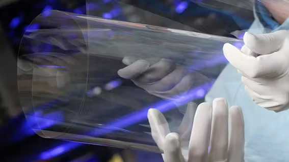
A metal mesh conductive film is a type of transparent conductive film material constructed by forming a micro-scale metallic grid pattern on a transparent substrate. This grid structure provides excellent electrical conductivity while maintaining high light transmittance. It is widely used in touchscreens, organic photovoltaics (OPV), transparent heating films, transparent antennas, and more.

Compared to traditional indium tin oxide (ITO), Metal Mesh exhibits superior conductivity, mechanical flexibility, and processing compatibility, making it especially suitable for bendable or large-sized devices.

1. Metal Grid Structure Design

The metal grid is the core component of Metal Mesh, where the grid lines act as conductive pathways. These grid patterns can be designed in squares, hexagons, or other geometric shapes. Key parameters of the grid include:

  • Line Width and Thickness: Wider and thicker metal lines improve conductivity but block more light, reducing transmittance.
  • Grid Pitch (Spacing): Smaller grid spacing provides more conductive pathways, enhancing electrical performance, but may sacrifice optical transparency.
  • Grid Shape: Hexagonal grids, for example, distribute current more evenly, reduce concentration effects, and improve structural uniformity.

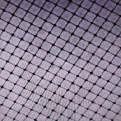
In different application scenarios, it is necessary to balance the trade-off between conductivity and transparency by reasonably designing grid parameters. For example, in touchscreen applications, the line width and spacing must ensure both good conductivity for touch signal transmission and high transmittance for display clarity.

2. Substrate Materials

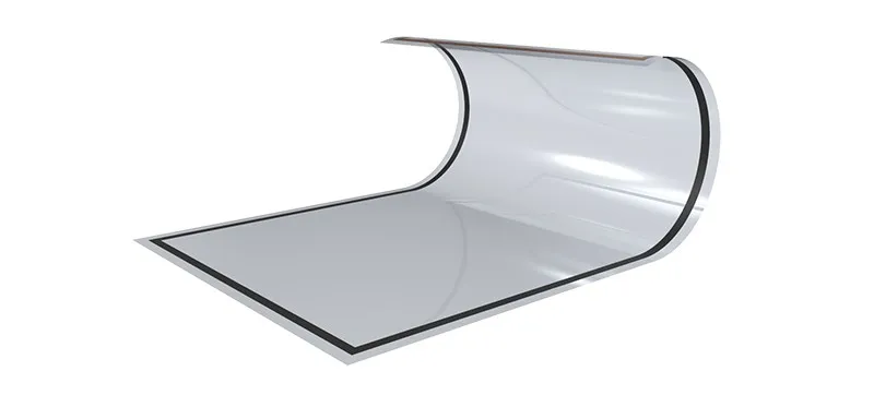
The substrate provides structural support for the metal grid. For flexible electronic devices, flexible plastic films are typically chosen as substrates to enable bending and stretching. Common flexible substrates include PET (polyethylene terephthalate), COP (cyclic olefin polymer), and PC (polycarbonate), each with unique properties such as thickness, heat resistance, and flexibility.

For applications requiring high flatness and hardness, glass substrates are more suitable.

What Factors Affect the Performance of Metal Mesh Conductive Films?

1. Material of the Metal Grid

  • Metal Type: Commonly used metals include silver (Ag), copper (Cu), and gold (Au). Silver offers excellent conductivity and optical properties; copper is cost-effective but prone to oxidation; gold provides high chemical stability and is used in high-end applications.
  • Purity: Higher-purity metals have lower resistance, improving overall conductive efficiency. Impurities increase electron scattering and raise resistance.

2. Structure of the Metal Grid

  • Grid Shape:
    • Square grids are structurally simple and easier to manufacture, with balanced conductivity in all planar directions.
    • Hexagonal grids (honeycomb-like) offer better spatial efficiency and more uniform conductivity in all directions, reducing current concentration.
  • Line Width and Thickness:
    Wider and thicker metal lines reduce resistance and improve conductivity but block more light. Narrower lines increase aperture ratio (open area) and transmittance.
  • Grid Pitch:
    Smaller spacing increases conductive path density and conductivity but reduces aperture ratio and transmittance.

3. Manufacturing Processes

  • Substrate Treatment:
    Surface treatments (e.g., cleaning, surfactant treatment) affect adhesion between the metal grid and substrate, impacting mechanical and electrical performance.
  • Deposition Process:
    • Physical Vapor Deposition (PVD): Methods like magnetron sputtering produce high-quality, dense metal films with strong substrate adhesion, low impedance, and high conductivity.
    • Chemical Vapor Deposition (CVD): Enables large-area, uniform films; conductivity can be optimized by controlling gas flow, temperature, and pressure.
    • Vacuum Evaporation: Requires precise control of temperature, pressure, and evaporation rate to ensure film uniformity and quality.
  • Patterning Process:
    Determines grid line integrity, uniformity, shape, and adhesion, significantly affecting conductivity, transmittance, and mechanical properties.
    • Photolithography Etching: Uses photoresist and etchants to create high-precision grids; complex and costly.
    • Laser Direct Writing: Directly engraves grid patterns with high precision/resolution; high equipment cost.
    • Nanoimprint Lithography: Transfers patterns using a stamp; suitable for large areas but requires high-precision templates.
  • Post-Treatment Processes:
    Processes like blackening, cleaning, surface modification, and annealing optimize electrical/optical performance. These reduce resistance, stabilize parameters, improve transmittance, minimize optical defects, and enhance chemical/mechanical stability (e.g., corrosion/oxidation resistance, stress relief).

MICRON’s Copper Metal Mesh Transparent Conductive Film

MICRON specializes in ultra-fine copper metal mesh (Metal Mesh) technology, forming grid structures with microscale metal traces to ensure high transmittance in transparent areas while achieving extremely low resistance.

Copper Metal Mesh Transparent Conductive Film

Our copper metal mesh films typically feature:

– High Transmittance: Achieved via fine-line patterning, ideal for transparent/visible applications.

– Low Sheet Resistance: Enabled by high-aspect-ratio traces.

– Flexibility/Bendability: Realized through film substrates and fine patterning.

– Wide Operating Temperature Range: -85°C to +85°C.

– High Design Freedom: Customizable grid designs based on application needs.

Conclusion

The performance of metal mesh conductive films depends on material properties, structural design, and manufacturing processes. By scientifically balancing parameters and processes, conductivity, transmittance, and mechanical properties can be optimized for diverse applications.

As a leader in this field, Zhiling Weiye has successfully applied Metal Mesh copper films in high-end sectors like touch displays, flexible electronics, automotive screens, and EMI shielding, driving industry innovation with outstanding performance.

For detailed application cases or sample requests, please feel free to contact us!

Homepage Product Dial up Message